MIPI-A1 ClockGen Calculator User Guide
References
Application version: 1.1.0
Document reference |
UG042 |
Document revision |
B |
Generation date |
26 Oct. 2026 |
Written by |
F. DESCAMPS |
23 Oct. 2026 |
Validated by |
- |
- |
Approved by |
K. TOUTAIN |
26 Oct. 2026 |
Related documents:
UG026MIPI-A1 Interface Board UserGuide, in particular section 9Renesas 5X2503 datasheet
Abbreviation table
CLI |
Command Line Interface |
GUI |
Graphical User Interface |
I2C |
Inter-Integrated Circuit |
LSB |
Least Significant Byte |
MSB |
Most Significant Byte |
PLL |
Phase-Locked Loop |
ppm |
Parts Per Million |
VCO |
Voltage-Controlled Oscillator |
Introduction
The MIPI-A1 ClockGen Calculator converts a target Proxy Board MasterClock into the four ClockGen register values to write on the FullScale MIPI-A1 Interface Board, and decodes an existing register set back into a frequency.
It is a calculation helper, not a programming tool: it never opens the I2C bus and is not connected to a board. The values it reports are to be written by whatever already drives the board, and the application also lists the configuration sequence they have to be written in.
Note
The application runs on Windows and on Debian-based Linux, Raspberry Pi OS included, with a graphical interface and a command line tool. This guide documents the graphical interface; Command line use covers the equivalent commands.
The clock chain
The MasterClock is generated by a Renesas 5X2503. PLL1 runs from the device’s integrated 26 MHz crystal and feeds Output Divider 1:
VCO         = 26 MHz * N / M
MasterClock = VCO / out_div
M, N and out_div are the only parameters the board exposes. The loop
filter, charge pump, spread spectrum and output routing are fixed in FPGA
firmware. The crystal is specified at 26 MHz ±20 ppm, which sets the accuracy
floor: no choice of dividers is more accurate than the reference.
The divider ranges the application searches are:
Parameter |
Range |
Notes |
|---|---|---|
|
1, 2, or 3 to 63 |
1 and 2 are the bypass paths, not integer divider values |
|
12 to 2047 |
11 bits; below 12 the PLL may not lock |
|
1 to 48 |
The product of a ×1/×2/×4/×8 and a ×1/×4/×5/×6 factor |
The registers
Four board registers hold the dividers. Each maps onto a 5X2503 configuration byte:
Board register |
5X2503 byte |
Field |
Holds |
|---|---|---|---|
|
Byte 08h |
bits 7, 6, 5:0 |
M divider, or a bypass |
|
Byte 0Ah[2:0] |
bits 2:0 |
N[10:8] |
|
Byte 09h |
bits 7:0 |
N[7:0] |
|
Byte 0Fh |
bits 7:6, 5:4 |
Output Divider 1 |
Warning
Bits 7:3 of 0x1311 belong to the PLL1 loop filter and must be 0. Only
bits 2:0 carry N[10:8].
Installation
Raspberry Pi OS and Debian
Install the provided package:
sudo apt install python3-tk           # required by the graphical interface
sudo dpkg -i db-mipi-a1-clockgen-1.0.deb
The package installs two commands:
Command |
Starts |
|---|---|
|
The graphical application |
|
The command line tool |
The application also appears in the desktop menu under FullScale Tools. If it is not there yet, log out and back in: the desktop menu is built at session start.
Windows
Run the provided installer, db-mipi-a1-clockgen-1.1.0-setup.exe, and start
MIPI-A1 ClockGen Calculator from the FullScale group of the Start menu.
The installer also offers a desktop shortcut. The executable is
self-contained: no Python installation is required.
Note
The Windows build is windowed and has no console, so it always starts the graphical interface.
The application window
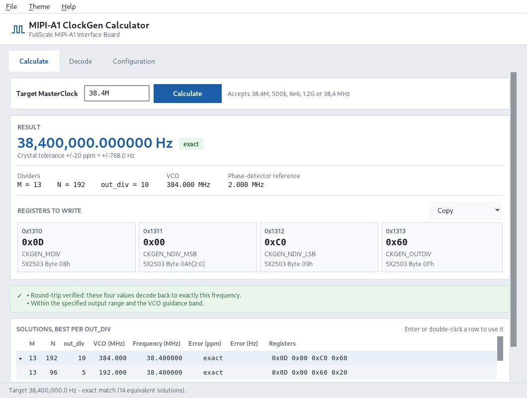
Figure 1: The window after calculating a 38.4 MHz target.
The window has four areas:
Area |
Contents |
|---|---|
Menu bar |
File, Theme and Help. See Menus, theme and shortcuts. |
Header |
Application name and the board it applies to. |
Tab strip |
Calculate, Decode and Configuration. |
Status bar |
The outcome of the last action, at the bottom of the window. |
The three tabs answer three different questions:
Tab |
Use it to |
|---|---|
Calculate |
Turn a target frequency into register values. |
Decode |
Find out what a register set already on a board produces. |
Configuration |
See the order the values must be written in. |
The window can be resized down to 880 × 560, and each tab scrolls if the window is too short for its contents. It is usable on an 800 × 480 Raspberry Pi touchscreen.
Calculating register values
Entering a target
Type the wanted MasterClock in Target MasterClock and press
Enter, or click Calculate. The field starts at 38.4M.
A target may be written in any of these forms:
Written as |
Read as |
|---|---|
|
Suffixed or exponent notation |
|
Comma as the decimal separator |
|
Grouped digits |
|
Plain hertz |
A value that cannot be read is refused: the field is outlined in red and the hint beside it is replaced by the reason. Nothing is calculated and the previous result is cleared, so a rejected entry can never be mistaken for a result.
Reading the result
The Result card reports, in reading order:
Field |
Meaning |
|---|---|
MasterClock |
The frequency the registers actually produce, to 6 decimals. |
Accuracy chip |
|
Crystal tolerance |
The ±20 ppm of the reference, in hertz at this frequency. Compare it with the error above: an error well inside the tolerance is not worth chasing. |
Dividers |
The |
VCO |
The PLL1 output frequency. |
Phase-detector reference |
26 MHz / |
Registers to write below shows the four bytes, each with its board address, register name and the 5X2503 byte it lands in. These are the values to program.
Warnings and confirmations
A callout under the result card reports the state of the solution. Green confirms that the values were checked; amber raises a point to verify.
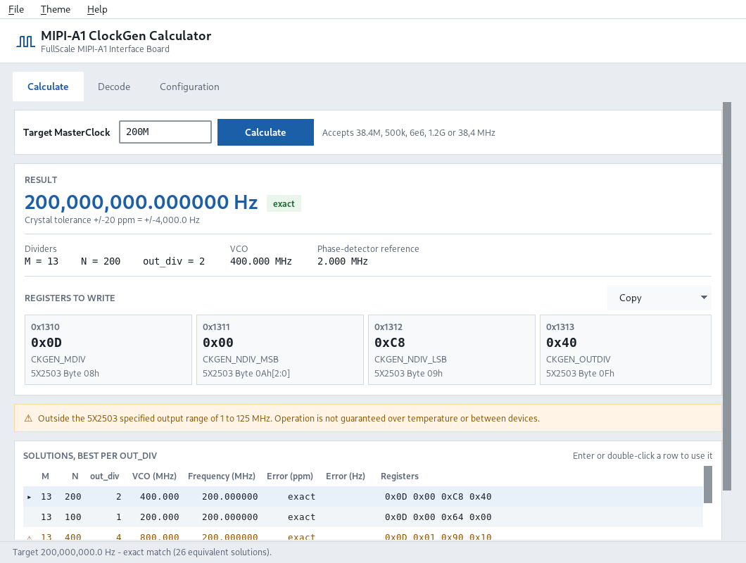
Figure 2: A 200 MHz target: reachable exactly, but outside the specified output range.
Callout |
Meaning |
|---|---|
Green |
The four values decode back to exactly this frequency, and the result is within the specified output range and the VCO guidance band. |
Amber |
The frequency is outside the 1 to 125 MHz specified output range, the VCO is outside the 0 to 700 MHz guidance band, or the closest reachable frequency is more than 0.1 % from the target. |
Red |
The register encoding does not reproduce the frequency. Do not program these values, and report the case. |
Note
Nothing is ever excluded on these grounds. A frequency outside the specified range is still calculated and reported, because it may still be the right choice for a bring-up; the warning says that operation is not guaranteed over temperature or between devices.
Choosing another solution
The same frequency is usually reachable with several divider combinations. Solutions, best per out_div lists the best one for each output divider, ranked best first:
Column |
Contents |
|---|---|
Marker |
|
M, N, out_div |
The dividers. |
VCO (MHz) |
The PLL1 frequency they give. |
Frequency (MHz) |
The MasterClock they produce. |
Error (ppm), Error (Hz) |
Distance from the target, or |
Registers |
The four bytes, in address order. |
Select a row and press Enter, or double-click it, to make it the active solution: the result card, the register values and the configuration sequence all follow. Hovering an out-of-band row shows why it is marked.
Choosing a different out_div is how to move the VCO while keeping the same
output frequency, which matters when the default lands outside the guidance
band or on an awkward operating point.
Copying the values
Copy, at the right of the register card, puts the active solution on the clipboard in one of six formats:
Format |
Produces |
|---|---|
Register list |
One address, name and value per line. Ctrl-C copies this one. |
C array |
An initialised |
C #defines |
An |
Python dict |
|
CSV |
A header row, then address, register, value and 5X2503 byte. |
I2C write sequence |
The four writes plus the whole start, poll and enable procedure, as comments and assignments that can be pasted into a session. |
Every format but the register list carries a comment line naming the frequency, the dividers and the accuracy, so a set of values pasted into a mail or an issue still says what it produces. A short confirmation appears in the card and in the status bar.
Decoding a register set
The Decode tab answers the opposite question: given four register values, what MasterClock does the board produce?
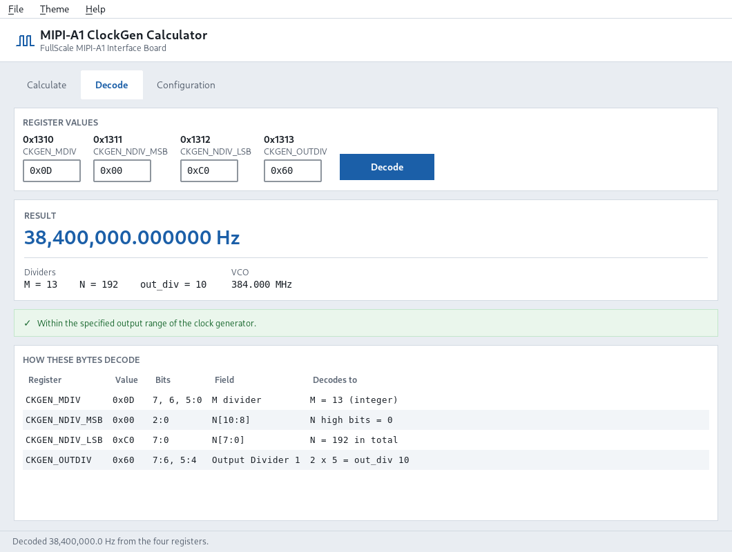
Figure 3: Decoding the register set of a 38.4 MHz MasterClock.
Enter the four bytes and press Enter, or click Decode. Each field
accepts 0x0D, 13 or 0b1101.
The result card gives the frequency, the dividers and the VCO. How these bytes decode below shows the derivation byte by byte: which bits were read, what field they are, and what they came to. The same nibble means a different thing in each register, so this is what makes a set checkable by hand.
A register set the hardware cannot hold is refused rather than decoded, in a dialog naming the reason:
Refused because |
Reason |
|---|---|
|
The value is not a valid encoding of any M. |
N = 0 |
The feedback divider cannot be zero; the PLL would have no output to divide. |
A field is not a byte |
Registers hold |
A set that decodes but is questionable is reported in the callout instead: bits
7:3 set in 0x1311, which belong to the loop filter, or an N below 12, where
the PLL may not lock.
Note
The command line refuses exactly the same sets, for the same reasons.
The configuration sequence
Writing the four registers is not enough to bring the clock up. The Configuration tab shows the whole procedure, with the values of the active solution in it.
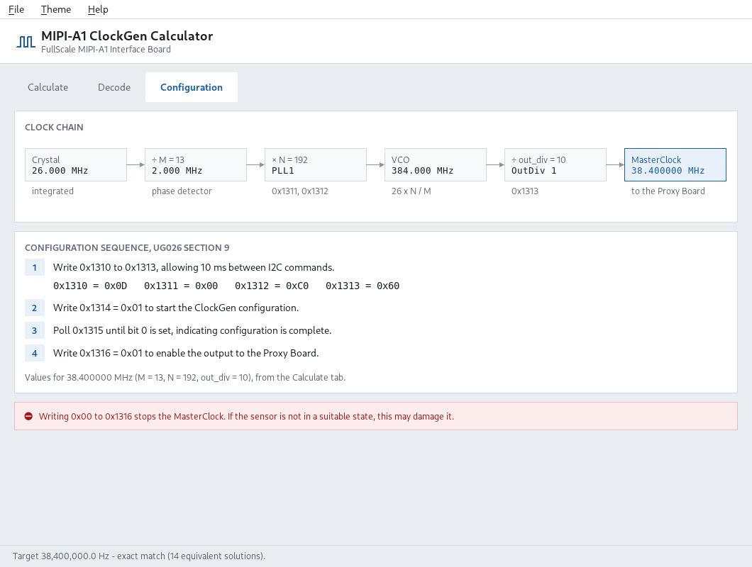
Figure 4: The configuration sequence, carrying the values from the Calculate tab.
Clock chain traces the crystal through the phase detector, the feedback divider, the VCO and the output divider to the MasterClock, annotated with the live values and the register that sets each stage.
Configuration sequence is UG026 section 9:
Write
0x1310to0x1313, allowing 10 ms between I2C commands. The values for the active solution are shown under this step.Write
0x1314 = 0x01to start the ClockGen configuration.Poll
0x1315until bit 0 is set, indicating configuration is complete.Write
0x1316 = 0x01to enable the output to the Proxy Board.
Danger
Writing 0x00 to 0x1316 stops the MasterClock. If the sensor is not
in a suitable state, this may damage it.
The I2C write sequence copy format contains this procedure with the values already in place.
Menus, theme and shortcuts
Menu |
Entries |
|---|---|
File |
Copy register values, and Quit. |
Theme |
Follow system, Light or Dark. |
Help |
About: version, the clock equations and the reference documents. |
The theme follows the desktop setting by default, and the system setting is re-checked while the application runs. Choosing Light or Dark pins it.
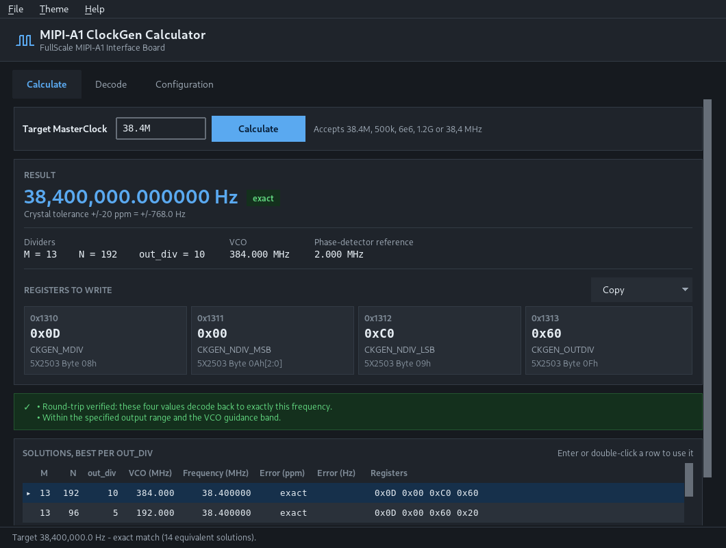
Figure 5: The same window in the dark theme.
Note
Changing theme rebuilds the window. The entered values and the open tab are carried across, so nothing typed is lost.
Every frequent action has a key:
Key |
Action |
|---|---|
Enter |
Calculate, or decode, from the field being edited. |
Ctrl-Enter |
Calculate, from anywhere in the window. |
Ctrl-C |
Copy the register values as a register list. |
Ctrl-L |
Put the cursor in the target field. |
Ctrl-1, Ctrl-2, Ctrl-3 |
Go to the Calculate, Decode or Configuration tab. |
Page Up, Page Down |
Scroll the current tab. |
F1 |
About. |
Ctrl-Q |
Quit. |
Command line use
Everything the window does is available on the command line, which is the form
to use in a script or over a remote session. The command line tool is
db-mipi-a1-clockgen-cli.
db-mipi-a1-clockgen-cli 38.4M                      # solve for a target
db-mipi-a1-clockgen-cli "38,4 MHz" --top 8         # list 8 alternatives
db-mipi-a1-clockgen-cli --decode 0x0D 0x00 0xC0 0x60
db-mipi-a1-clockgen-cli --version
Targets are written in the same forms the window accepts. The output gives the recommended solution, its register values, the alternatives and the configuration sequence:
Target: 38400000.000000 Hz (38.400000 MHz)

Recommended:
  M = 13   N = 192   out_div = 10
  VCO = 384.000 MHz   phase-detector reference = 2.000 MHz
  MasterClock = 38400000.000000 Hz  (exact; crystal tolerance +/-20 ppm = +/-768.0 Hz)

    0x1310  CKGEN_MDIV      = 0x0D      5X2503 Byte 08h
    0x1311  CKGEN_NDIV_MSB  = 0x00      5X2503 Byte 0Ah[2:0]
    0x1312  CKGEN_NDIV_LSB  = 0xC0      5X2503 Byte 09h
    0x1313  CKGEN_OUTDIV    = 0x60      5X2503 Byte 0Fh
The options are --top N for the number of alternatives, --vco-nominal
for the preferred VCO when several solutions are exact, --vco-max for the
value above which a VCO is annotated, and --decode for a register set.
Warnings are printed as WARNING: lines and refusals as ERROR: lines on
standard error. The exit status is 0 on success, 1 when no solution exists or a
register set cannot be decoded, and 2 when an argument could not be read.
The graphical interface is started with db-mipi-a1-clockgen. Both
commands have a manual page:
man db-mipi-a1-clockgen-cli
man db-mipi-a1-clockgen
Messages and limits
Message |
What it means |
|---|---|
Not a frequency. Try 38.4M, 500k, 6e6 or 38,4 MHz. |
The target could not be read. The accepted forms are listed in Command line use and above. |
No solution within the divider ranges |
No combination of M, N and |
Outside the 5X2503 specified output range of 1 to 125 MHz |
The result is reported and usable, but operation is not guaranteed over temperature or between devices. |
VCO falls outside the guidance band |
PLL1’s operating range is not published; the 0 to 700 MHz band is used
only to rank solutions. Verify the output on hardware, or pick another
|
Closest reachable frequency is more than 0.1 % from the target |
The divider ranges cannot land nearer. Check whether the sensor tolerates it. |
Nothing to copy: calculate a target first |
Copy acts on the active solution, and there is none yet. |
Two limits are worth keeping in mind when reading any result:
The 26 MHz crystal is specified at ±20 ppm, so no result is more accurate than that, whatever the solve error says.
M,Nandout_divare the only parameters the board exposes. Everything else in the 5X2503 is fixed in FPGA firmware and cannot be changed from this application.
Revision history
Date |
Author(s) |
Version |
Comments |
|---|---|---|---|
08/2026 |
F. DESCAMPS |
Rev. A |
First document release |
10/2026 |
F. DESCAMPS |
Rev. B |
Version 1.1.0: installer name, disclaimer typos |